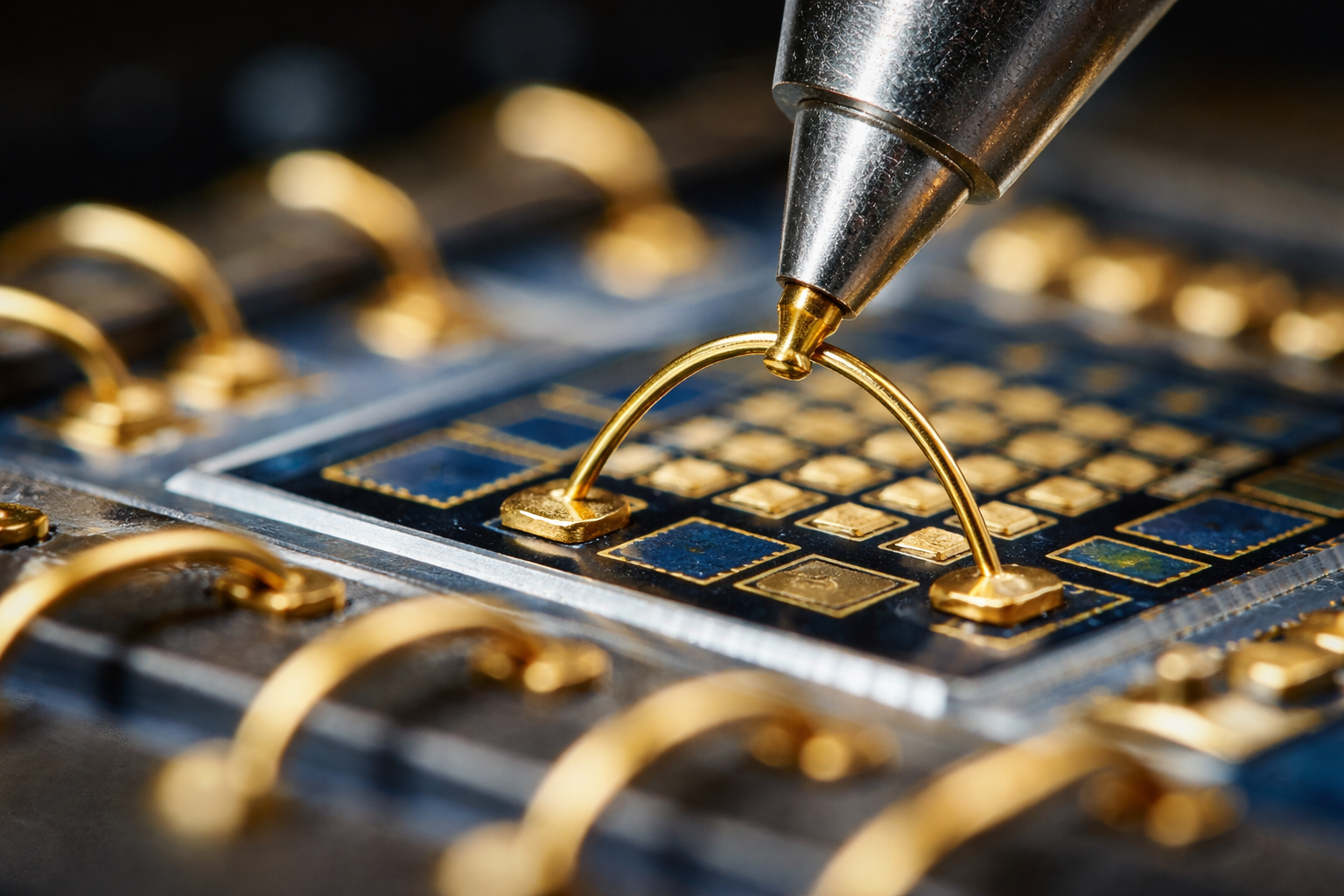
The demand for advanced IC packaging bonding solutions is on the rise as industries seek to improve product performance and efficiency. The wire bonding market is projected to reach approximately 4.79 billion USD by 2025, reflecting a strong CAGR of 5.6% as outlined in recent industry forecasts. This growth is pivotal, particularly as manufacturers focus on semiconductor wire bonding technology to enhance the IC packaging wire bonding process. The increasing need for reliable connections in microelectronics has led to significant advancements in bonding equipment and techniques, fostering a competitive landscape rich with opportunities.
Key industry participants such as Hesse Mechatronics (DE), Shinkawa Ltd. (JP), and Palomar Technologies, Inc. (US) are driving innovation in the IC packaging sector. These companies are at the forefront of developing solutions that integrate microelectronics bonding equipment with next-generation semiconductor wire bonding technology. Their commitment to research and development is evident as they push boundaries to create efficient bonding processes that meet evolving market demands. As these players continue to innovate, the market is expected to benefit from enhanced productivity and improved yield rates. The development of IC packaging bonding solutions continues to influence strategic direction within the sector.
Factors contributing to the growth of IC packaging bonding solutions include the surge of consumer electronics requiring high-density packaging and the ongoing miniaturization trend across devices. Additionally, developments in automotive electronics, particularly electric vehicles, have spurred increased demand for efficient and reliable bonding solutions. However, challenges persist, including the need to manage rising costs of materials and the complexity of integrating new technologies into existing production lines. Companies must navigate these hurdles to maintain competitiveness and capitalize on the growing opportunities within the market.
North America continues to dominate the wire bonding market, owing to its robust semiconductor ecosystem, while the Asia-Pacific region emerges as a hotspot for growth. Countries such as China and Japan are heavily investing in manufacturing capabilities, leading to a rapid increase in demand for innovative IC packaging bonding solutions. As these regions strengthen their positions, they pave the way for significant advancements in microelectronics bonding technology, attracting further investments to meet local and global demand.
In terms of market figures, the Asia-Pacific region is projected to experience a CAGR of 6.5% from 2020 to 2025, driven by substantial investments in semiconductor manufacturing and a growing consumer electronics market. The increasing adoption of smart devices and IoT applications in this region is expected to further escalate demand for advanced bonding solutions. For instance, China’s investment in its semiconductor industry reached approximately 150 billion USD in 2021, indicating the government’s commitment to becoming a global leader in this sector. Real-world examples of successful integration of wire bonding technology can be seen in companies like Samsung and TSMC, which have leveraged advanced bonding techniques to enhance the performance of their chips, resulting in higher yields and better energy efficiency.
The wire bonding market is poised for robust growth, propelled by advancements in semiconductor wire bonding technology and the increasing adoption of microelectronics bonding equipment. Investment in R&D is critical, as companies seek to innovate and provide enhanced IC packaging bonding solutions. Furthermore, the move towards sustainable manufacturing practices is creating new avenues for growth, as firms aim to lessen their environmental footprint while improving efficiency and reliability.
Looking ahead to 2035, the Wire Bonding Market is expected to witness continued expansion, driven by innovation and increasing demand for high-performance bonding solutions. Market Research Future indicates that ongoing advancements in technology and consumer preferences will shape the competitive landscape, prompting companies to invest significantly in R&D. Collaborations and strategic partnerships will be fundamental in navigating market challenges and ensuring sustainable growth within the sector.
AI Impact Analysis
The integration of AI and machine learning into the IC packaging bonding process is revolutionizing manufacturing practices. By analyzing large data sets, AI can enhance the precision of the bonding process, leading to reduced waste and improved yield rates. These technologies also enable predictive maintenance of microelectronics bonding equipment, allowing for real-time adjustments and optimizations to enhance operational efficiency.
Frequently Asked Questions
Electric Lighting Equipment Market
Electrical Electronic Test Equipment Market
Electrical Test Equipment Market
Electron Microscopy Sample Preparation Market
Electronic Components For Hvdc System Market